
Feb 27, 2013Researchers at North Dakota State University (NDSU) have developed a method for embedding ultrathin passive radio frequency identification chips on paper or other flexible substrates. This method, the team reports, could enable the production of RFID-enabled paper at a cost lower than that pertaining to traditional RFID tags. The group is now seeking manufacturing partners to help commercialize the technology.
The process, known as Laser Enabled Advanced Packaging (LEAP), involves silicon chips so thin that they would not be detected when embedded in a piece of paper. The chips, along with antennas, are joined on a substrate at high speed, using a low-cost laser technology. Products that the method could create include security and financial paper, such as banknotes, legal documents, tickets and smart labels—all of which could benefit from having the RFID technology built into them, by proving an item's authenticity, and thereby preventing counterfeiting.
While there are RFID-based paper solutions on the market, says Val Marinov, an associate professor at NDSU and the head of the LEAP project, most RFID chips are not thin enough to be integrated into paper without either requiring the paper to be thicker than desired, or creating a bump on its surface that could interfere with printing. To be embedded in an average piece of paper without creating a significant bump, he explains, the technology would require a chip that is 20 microns (0.0008 inch) or thinner. "Thinner also means more reliable," Marinov says, adding, "At such small thicknesses, the silicon—which is otherwise a very brittle material—becomes flexible and capable of extreme bending."
Currently, Marinov says, few RFID chips are that thin, and the methods to assemble them into tags or paper are limited. Traditional pick-and-place solutions lack the speed or precision required to assemble the chip on a substrate at a low cost. When the chips are small enough, the gravitational force exerted on them is limited, and surface forces of attraction—such as static electricity—can thus make it difficult to release the chips. As such, contact assembly methods, such as the pick-and-place approach, fail as a high-precision, high-volume solution for ultrasmall, ultrathin chips.
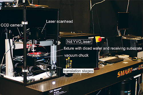
Therefore, the NDSU researchers have developed a process for assembling ultrathin, ultrasmall chips, and have built a prototype of a solution capable of embedding ultrasmall RFID chips onto a paper substrate. The system employs a plasma etcher to thin silicon wafers down to size, if necessary, and to cut the wafers, as well as a laser beam to transfer each chip onto a substrate.
Once the inlay is ready for assembly, an ultraviolet (UV) laser pulse is directed at the DRL bonding material holding the die, thereby creating a blister. The force exerted by the blister causes the contactless die to transfer from the wafer onto the receiving substrate (the system includes a camera that allows for proper alignment of the laser beam), where the chip is connected to the antenna pads. The substrate can then be laminated to a second sheet of paper, thereby embedding the chip and antenna in the paper, which can then be used to manufacture banknotes or other paper items.

To test the technology, researchers required a passive ultrahigh-frequency (UHF) EPC RFID chip thinner than those currently available off the shelf. The team used a 750-micron (0.03-inch)-thick wafer of uncut Alien Technology Higgs 3 chips that they mechanically ground down to a thickness of approximately 65 microns (0.003 inch); at the time, the group had not yet mastered the process of thinning beyond 65 microns. During a second test, however, they ground a wafer of uncut dummy silicon chips (not RFID ICs) down to 50 microns (0.002 inch) in thickness, an then further thinned them to 20 microns (0.0008 inch) via plasma etching (the second part of the thinning process was performed with etching in order to minimize the risk of damaging the chip).
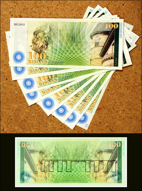
During both tests, the wafer was then bonded to the carrier adhesive, and was cut into chips that were transferred to the paper substrate using the LEAP laser-based method. The substrate containing the chip and antenna was embedded in paper the size of a banknote. The paper was then read using an Alien ALR-9650 RFID reader. Nine of 10 samples could be interrogated using the reader, Marinov says.
Not only is the LEAP manufacturing process more precise, Marinov says, but it can also be performed much more quickly than traditional pick-and-place methods. He estimates that packaging chips on substrates can be completed at least twice as fast as is possible via traditional methods, since multiple dies can be transferred almost simultaneously in parallel to a single large sheet of paper by moving the laser beam very quickly over each chip to be transferred. The large paper sheet would then be cut into individual pieces, each embedded with its own RFID chip and antenna. The increase in throughput, he notes, can be achieved without increasing equipment expenses.
The group spent approximately the past four years researching the RFID industry, the need for RFID-enabled paper for counterfeit prevention and existing assembly methods, Marinov says—and, in so doing, proved LEAP's feasibility and built a prototype to accomplish the LEAP assembly method. "We spent quite a bit of time understanding the problem," he states.
The researchers first demonstrated the technology in 2011. Now, the group is seeking commercial partners to help bring the technology to market. Such partners might be RFID tag manufacturers or equipment makers for the actual chip-packaging process. "We're open to all kinds of collaborations," Marinov says, adding that while there are a few RFID chips commercially available that are small enough to be embedded in paper, none are as thin as 20 microns, while the LEAP method would enable manufacturers to etch silicon wafers down to a thinner size.
The market for RFID-enabled paper may be broad, Marinov says, but it is also difficult to measure. Because such a solution isn't readily available, he adds, it isn't being used at present. Use cases might exist, however, such as building RFID technology into concert or transportation tickets, to be read when a ticket is redeemed, in order to prove its authenticity. If the RFID-enabled paper were used to produce banknotes, the tags could be employed to prove a note's authenticity. Legal documents could also enable users to capture or store data via an RFID reader that would prove the document was not counterfeit.
According to Marinov, the LEAP method also works for assembling other types of ICs and small components, in addition to RFID chips. For example, LEAP could be used to assemble light-emitting diodes (LEDs) and micro-electrical mechanical systems (MEMS) components.
